Nordic nRF52833 BLE 5.2 module chip antenna long distance AoA AoD module
RF-BM-ND07 is an RF module based on Nordic BLE SoC nRF52833QIAA with ARM? Cortex?-M4 32-bit processor. It integrates a 32.768 kHz and a 32 MHz crystal, an LC filter, an antenna matching and a meander line chip antenna. It features low power consumption, small size, robust connection distance, and rigid reliability. It supports Bluetooth 5.2 Low Energy, Bluetooth mesh, NFC, Thread and Zigbee. It includes a range of analog and digital interfaces such as NFC-A, ADC, full-speed 12 Mbps USB 2.0, High-speed 32 MHz SPI, UART / SPI / TWI, PWM, I2S and PDM, which make this module an ideal device for a wide range of commercial and industrial applications, including professional lighting, asset tracking, advanced wearables or smart home applications where robust coverage is important.
Parameters of RF-BM-ND07
Chipset | nRF52833QIAA |
Supply Power Voltage | 1.7 V ~ 5.5 V, recommended to 3.3 V |
Frequency | 2402 MHz ~ 2480 MHz |
Transmit Power | -20.0 dBm ~ +8.0 dBm (Typical: 0 dBm) |
Receiving Sensitivity | -103 dBm @ 125 kbps BLE -96 dBm @ 1 Mbps BLE |
GPIO | 42 |
Crystal | 32 MHz |
RAM | 128 KB |
Flash | 512 KB |
Package | SMT Packaging |
Frequency Error | ±20 kHz |
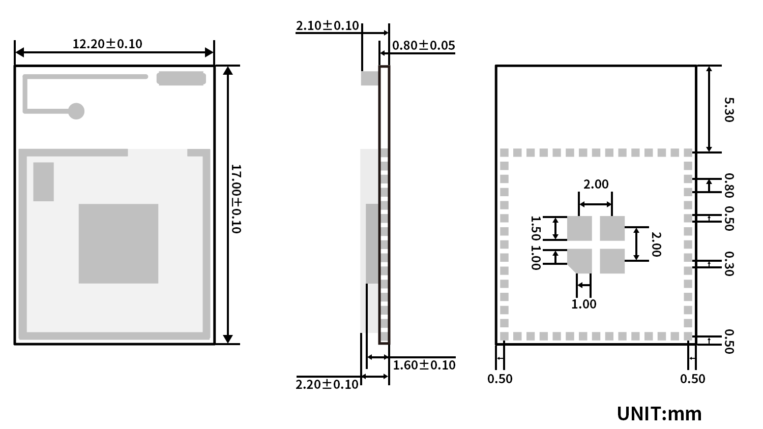
Dimension | 12.2 mm x 17.0 mm x (2.2 ± 0.1) mm |
Type of Antenna | Chip antenna |
Operating Temperature | -40 ℃~ +85 ℃ |
Storage Temperature | -40 ℃~ +125 ℃ |


Recommended Footprint
Pin Attributes
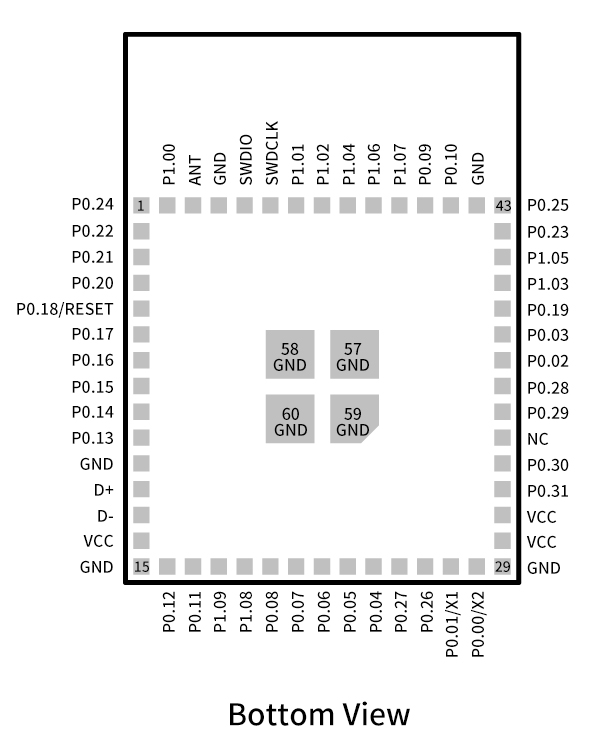
Pin Functions of RF-BM-ND07
Pin | Name | Pin Type | Description |
1 | P0.24 | Digital I/O | General purpose I/O |
2 | P0.22 | Digital I/O | General purpose I/O |
3 | P0.21 | Digital I/O | General purpose I/O |
4 | P0.20 | Digital I/O | General purpose I/O |
5 | P0.18 | Digital I/O | General purpose I/O |
| nRESET |
| Configurable as pin RESET |
6 | P0.17 | Digital I/O | General purpose I/O |
7 | P0.16 | Digital I/O | General purpose I/O |
8 | P0.15 | Digital I/O | General purpose I/O |
9 | P0.14 | Digital I/O | General purpose I/O |
10 | P0.13 | Digital I/O | General purpose I/O |
11 | GND | Ground |
|
12 | D+ | USB | USB D+ |
13 | D- | USB | USB D- |
14 | VCC | VCC | Power supply: 1.7 V ~ 5.5 V , recommended to 3.3 V. |
15 | GND | Ground |
|
16 | P0.12 | Digital I/O | General purpose I/O |
| TRACEDATA1 | Trace data | Trace buffer TRACEDATA[1] |
17 | P0.11 | Digital I/O | General purpose I/O |
| TRACEDATA2 | Trace data | Trace buffer TRACEDATA[2] |
18 | P1.09 | Digital I/O | General purpose I/O |
| TRACEDATA3 | Trace data | Trace buffer TRACEDATA[3] |
19 | P1.08 | Digital I/O | General purpose I/O |
20 | P0.08 | Digital I/O | General purpose I/O |
21 | P0.07 | Digital I/O | General purpose I/O |
| TRACECLK | Trace clock | Trace buffer clock |
22 | P0.06 | Digital I/O | General purpose I/O |
23 | P0.05 | Digital I/O | General purpose I/O |
| AIN3 | Analog input | Analog input |
24 | P0.04 | Digital I/O | General purpose I/O |
| AIN2 | Analog input | Analog input |
25 | P0.27 | Digital I/O | General purpose I/O |
26 | P0.26 | Digital I/O | General purpose I/O |
27 | P0.01 | Digital I/O | General purpose I/O |
| XL2 | Analog input | Connection for 32.768 kHz crystal |
28 | P0.00 | Digital I/O | General purpose I/O |
| XL1 | Analog input | Connection for 32.768 kHz crystal |
29 | GND | Ground |
|
30 | VCC | VCC |
|
31 | VCC | VCC |
|
32 | P0.31 | Digital I/O | General purpose I/O |
| AIN7 | Analog input | Analog input |
33 | P0.30 | Digital I/O | General purpose I/O |
| AIN6 | Analog input | Analog input |
34 | NC | - |
|
35 | P0.29 | Digital I/O | General purpose I/O |
| AIN5 | Analog input | Analog input |
36 | P0.28 | Digital I/O | General purpose I/O |
| AIN4 | Analog input | Analog input |
37 | P0.02 | Digital I/O | General purpose I/O |
| AIN0 | Analog input | Analog input |
38 | P0.03 | Digital I/O | General purpose I/O |
| AIN1 | Analog input | Analog input |
39 | P0.19 | Digital I/O | General purpose I/O |
40 | P1.03 | Digital I/O | General purpose I/O |
41 | P1.05 | Digital I/O | General purpose I/O |
42 | P0.23 | Digital I/O | General purpose I/O |
43 | P0.25 | Digital I/O | General purpose I/O |
44 | GND | Ground |
|
45 | P0.10 | Digital I/O | General purpose I/O |
| NFC2 | NFC input | NFC antenna connection |
46 | P0.09 | Digital I/O | General purpose I/O |
| NFC1 | NFC input | NFC antenna connection |
47 | P1.07 | Digital I/O | General purpose I/O |
48 | P1.06 | Digital I/O | General purpose I/O |
49 | P1.04 | Digital I/O | General purpose I/O |
50 | P1.02 | Digital I/O | General purpose I/O |
51 | P1.01 | Digital I/O | General purpose I/O |
52 | SWDCLK | Debug | Serial wire debug clock input for debug and programming |
53 | SWDIO | Debug | Serial wire debug I/O for debug and programming |
54 | GND | Ground |
|
55 | ANT | RF | Single-ended radio antenna connection |
56 | P1.00 | Digital I/O | General purpose I/O |
| TRACEDATA0 | Trace data | Trace buffer TRACEDATA[0] |
57 | GND | Ground |
|
58 | GND | Ground |
|
59 | GND | Ground |
|
60 | GND | Ground |
|